What is Transistor?
Answer :- Transistor is a semiconductor device that can both conduct and insulate. A transistor can act as a switch and an amplifier. It converts audio waves into electronic waves and resistor. Controlling electronic current.
- A transistor has three doped regions forming two p-n junction between them.
Types of Transistor :-
There are two types of Transistor –
(1) N-P-N transistor.
(2) P-N-P transistor.
N-P-N Transistor :-
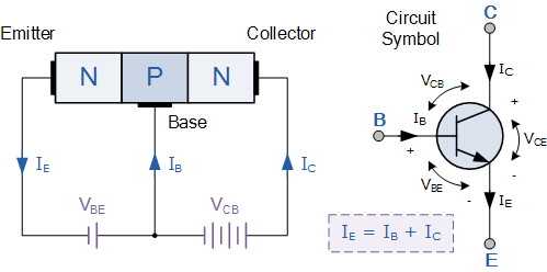
Here two segments of N-type semiconductor (emitter and collector) are separated by a segment of P-type semiconductor (base).
Emitter :-
This is the segment on one side of the transistor. It is of moderate size and heavy doped. It supplies a large number of majority carriers for the current flow through the transistor.
Collector :-
This segment collects a major portion of the majority carriers supplied by the emitter. The collector side moderately doped and larger in size as compare to the emitter.
Base :-
This is the central segment. It is very thin and lightly doped.
Working of N-P-N Transistor :-

- The collector and the base circuit is connected in reverse biased while the emitter and based circuit is connected in forward biased. The collector is always connected to the positive supply and the base is in negative supply for controlling ON/OFF states of the transistor.
- The forward biased voltage is small as compared to the reverse bias voltage.
- When the forward bias is applying across the emitter, The majority charge carriers move towards the base. This causes the emitter current. The electrons enter into the P-type material and combine with the holes.
- The base is tightly doped, Due to which only a few electrons are combined and remaining constitutes the base current. This base current enter into the collector region.
- If we represent the hole current and the electron current crossing the forward biased junction by Iₕ and Iₑ respectively then the total current in a forward biased is the sum of Iₕ and Iₑ
e.i.
Iₑₘᵢₜₜₑᵣ = Iₕ + Iₑ
- The current emerging from the base terminal and that form collector then froma straight forward application of Kirchhoff’s law, the emitter current is sum of collector current and base current.
P-N-P Transistor :-
- Here two segments of P-type semiconductor (emitter and collector) are separated by a segment N-type semiconductor.
- The segment emitter on one side, collector on another side of the transistor while segment base on central region.
Working of P-N-P Transistor :-

- Here the base terminal has negative bias with respect to emitter and the emitter terminal has positive bias voltage with respect to both the base and collector because of P-N-P transistor.
- The polarities and current directions are reversed here compared to N-P-N transistor. If the transistor is connected to all the voltage sources then the base current flows through the transistor but here the base voltage needs to be more negative with respect to the emitter to operate transistor. Here the base emitter junction acts as a diode.
- Here the base terminal acts as input and the emitter collector region acts as output.
Note :- The description about the paths followed by the majority and minority carriers in a P-N-P is exactly the same as that for the N-P-N transistor, but the current paths are exactly opposite. In the active state of the transistor the emitter-base junction acts as a low resistance while the base collector acts as a high resistance.
Basic transistor circuit configuration :-
In a transistor, only three terminals are available – emitter, base and collector. Therefore, in a circuit the input/output connections have to be such that one of these is common to both the input and output.
Accordingly, the transistor can be connected in either of the following three configurations –
(1) Common Emitter (CE)
(2) Common Base (CB)
(3) Common Collector (CC)

- The transistor is most widely used in common emitter configuration and more commonly used transistors are N-P-N-si transistors.
common Emitter Transistor Characteristics :-
When a transistor is used in common emitter configuration, the input is between the base and the emitter, the output is between the collector and the emitter.
- The variation of the base current with the base emitter voltage is called the input characteristic. similarly, the variation of the collector current with the collector-emitter voltage is called the output characteristic.
- The input and output characteristics of an N-P-N transistors can be studied by using the following circuit.

- To study the input characteristics of the transistor in CE configuration, a curve is plotted between the base current against the base Emitter voltage.

The collector-emitter voltage is kept fixed while studying the dependence of base current on base-emitter voltage. When the transistor is in active state, the collector-emitter voltage is kept large enough to make the base collector junction reverse biased.
- The output characteristic is obtained by observing the variation of collector current as collector-emitter voltage is varied keeping base current constant. If base-emitter voltage is increased by a small amount, both hole current from the emitter region and the electron current from the base region will increase. As a consequence both base current and collector current will increase opener proportionately.

Uses of Transistor :-
Transistor as a device :-
A transistor can be used as a device application depending on the configuration used (namely common base, common collector and common emitter), the biasing of the emitter-base and the base-collector junction and the operation region namely cutoff, active region and saturation.
- When the transistor is used in the cutoff or saturation state it acts as a switch. On the other hand for using the transistor as an amplifier, it has to operate in the active region.


